Plasma Nano-Processing
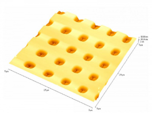
Nano-patterning of materials by plasma etching is an important technology in the semiconductor industry and will likely be called upon in the future for a range of applications in nano-technology. A new technique is being developed for massively parallel nanopatterning over large areas at an unprecedented small scale. A broad ion beam is directed at an array of micro-electrostatic lenses on a substrate. Voltages applied to the lenses focus the “beamlets” to spots that, when the substrate is tilted, write identical nano-features on the substrate.
Research Faculty

Vincent Donnelly
Professor of Chemical and Biomolecular Engineering
Faculty Web Page
Demetre Economou
Professor and Associate Chairman of Chemical and Biomolecular Engineering
Faculty Web Page

Paul Ruchhoeft
Associate Professor
Faculty Web Page