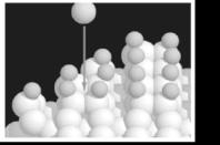
As dimensions continue to shrink, and as new devices with nanosize features emerge, traditional reactive ion etching results in electrical damage of sensitive devices. We have developed a new methodology that uses fast neutrals, instead of ions, to provide damage-free directional etching of nanoscale features. Fast neutrals are produced by simultaneous extraction and neutralization of plasma-generated ions through a grounded metal grid with high aspect ratio holes. Current work focuses on neutral beam characterization and etching of deep sub-50 nm features.
As device dimensions shrink to 10s of nm, film deposition and etching with monolayer accuracy must be developed. We are developing a new atomic layer etching method for damage-free etching with atomic resolution. By alternating between reactant chemisorption and “chemical sputtering” product removal steps, the required number of atomic layers of a solid are etched away, in a self-limiting process. Molecular dynamics simulations are used to guide experimentation aimed at testing the ultimate limit of feature size that may be fabricated.
Research Faculty

