Plasma Nano-Processing
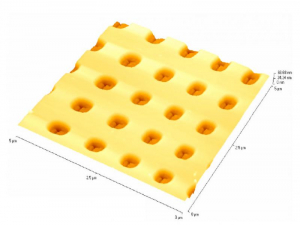
Nano-patterning of materials by plasma etching is an important technology in the semiconductor industry and will likely be called upon in the future for a range of applications in nano-technology. A new technique is being developed for massively parallel nanopatterning over large areas at an unprecedented small scale. A broad ion beam is directed at an array of micro-electrostatic lenses on a substrate. Voltages applied to the lenses focus the “beamlets” to spots that, when the substrate is tilted, write identical nano-features on the substrate.
Research Faculty

Vincent Donnelly
Moores Professor

Demetre Economou
Professor, Post-Tenure

Paul Ruchhoeft
Associate Professor