Plasma processing is an important technology for many industries including semiconductor integrated circuits, textiles, jet engines, and artificial joints. Our research group studies plasma processes used to etch and deposit microelectronics materials used today, as well as those that are being explored for future applications.
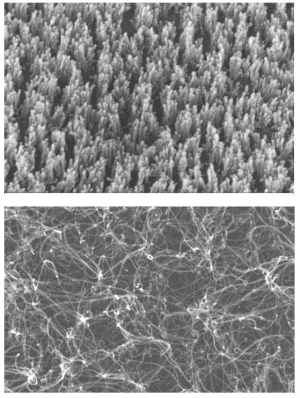
Plasma assisted chemical vapor deposition in a hydrocarbon, hydrogen plasma can lead to growth of amorphous carbon, or multi-walled carbon nanotubes that grow either vertically aligned or in random directions, depending on plasma conditions.
Hafnium oxide is replacing SiO2 as the dielectric layer below gate electrodes in integrated circuit transistors. We are investigating etching of this important material in boron trichloride plasmas, using diagnostic methods, including x-ray photoelectron spectroscopy (XPS). Etching in a BCl3 plasma successfully removes the HfO2 layer, but leaves an undesirable boron residue on the underlying silicon substrate. We can successfully remove this layer with a subsequent hydrogen plasma cleaning process.
Some of the most important, yet least understood aspects of plasma processing of materials are reactions at the reactor walls. These elusive processes have been difficult to study in the harsh plasma environment. We have developed a novel spinning substrate method to bring the surface from the plasma to an analysis chamber in less than 1 millisecond, where mass spectrometry detects heterogeneous reaction products desorbing, while Auger spectroscopy senses species that remain on the surface. By varying the rotation frequency, surface reaction kinetics can be determined.
Research Faculty